

Define input range and load behavior before choosing a part
Include adapter tolerance, cable loss, battery discharge, start-up current and rapid load steps. A microcontroller sleeping at microamp levels but drawing hundreds of milliamps during radio activity cannot be assessed using average current alone. Absolute maximum ratings are survival boundaries, not normal design targets.
An LDO drops excess voltage across a controlled pass device. A buck converter uses switching and energy storage to reduce voltage. Both can provide a lower rail, but neither a conventional buck nor an LDO can maintain a higher output when the source falls below it. A battery range that crosses the required rail may call for another topology, such as buck-boost, after a separate review.
- Specify the lowest and highest continuous input voltages.
- Record sleep, normal and peak output currents separately.
- Define output tolerance, permitted ripple and transient deviation.
- Identify enclosure temperature, board area and sensitive circuits.
Calculate LDO loss: 5 V in, 3.3 V out
A useful first estimate is P = (Vin − Vout) × Iout. Regulating 5 V to 3.3 V at 0.2 A produces approximately 0.34 W of heat in the LDO. Output power is 0.66 W, giving about 66 percent efficiency when quiescent current is neglected. This is an initial comparison, not a complete prediction of the device temperature.
For illustration, a junction-to-ambient resistance of 100 °C/W implies a 34 °C rise from 0.34 W. The actual rise depends on package, copper, layers, airflow and nearby heat. Datasheet resistance refers to specified test conditions. Confirm temperature in the intended enclosure before accepting the calculated dissipation.
| Example condition | Approximate LDO loss | Design implication |
|---|---|---|
| 5 V → 3.3 V, 20 mA | 0.034 W | A simple low-load solution may be suitable |
| 5 V → 3.3 V, 200 mA | 0.34 W | Review package and PCB heat flow |
| 12 V → 3.3 V, 200 mA | 1.74 W | The voltage difference creates much more heat |
Assess buck efficiency and layout as one design problem
A buck may offer lower loss as voltage difference or current increases. Peak advertised efficiency does not apply at every input and load: read matching curves. Light-load mode, switching frequency, inductor loss and external components affect the result. Avoid one assumed efficiency figure for every operating condition.
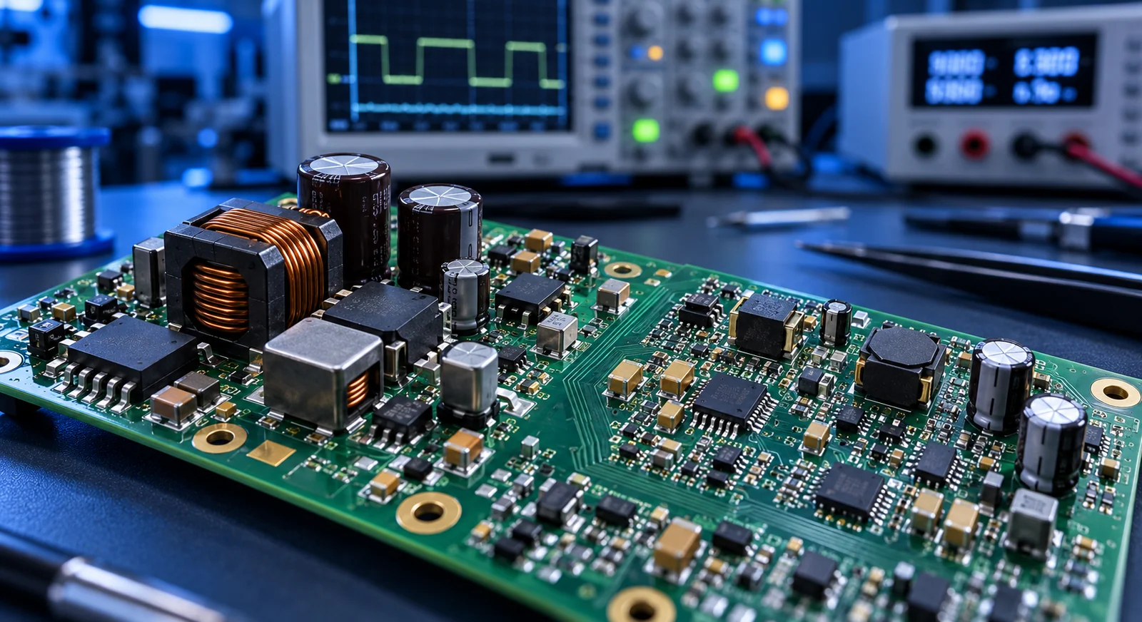
The high-current loops, input capacitor location, switching node and feedback routing require deliberate placement. Excessive switching-node copper or a feedback trace near a noisy route can undermine a correct schematic. Start with the selected manufacturer’s layout and component guidance. Verify both load-step response and output ripple on the actual PCB, including the operating modes the finished product will use.
Check dropout, capacitor requirements and power sequencing
An LDO needs sufficient input-to-output headroom to stay in regulation. Dropout changes with current and temperature, so review the relevant limits rather than relying on a headline typical value. A source barely above 3.3 V can lose the necessary margin through cable resistance or battery discharge. An LDO cannot boost the voltage when that margin disappears.
Capacitance, ESR and placement affect control-loop stability. Account for reduced effective ceramic capacitance under DC bias. Review enable sequencing, another supply driving the output and possible reverse current. Check start-up and shutdown alongside steady operation, especially when several rails feed a processor or sensor.
For batteries, include the current the regulator consumes
Quiescent current is the regulator’s own operating consumption; it is different from shutdown current. A contribution that seems small beside a 200 mA active load can dominate a sensor that sleeps for most of its life. Compare the selected parts at the relevant load and operating mode rather than treating the labels “LDO” and “buck” as sufficient evidence.
For example, a board sleeping at 10 µA with another 20 µA used by its regulator has a significant regulator contribution. These figures illustrate a budget, not a particular component. Include dividers, indicators, protection and sensors. Combine sleep and active durations, radio bursts, usable battery capacity and temperature in the estimate.
Consider buck plus LDO for rails with different priorities
A buck can feed digital loads while a downstream LDO supplies sensitive analog circuits. Leave sufficient headroom, calculate LDO loss and inspect PSRR at relevant frequencies. An LDO does not remove every switching artifact; adding one without checking conditions can simply add heat and components.
Compare temperature, sleep consumption, load-step response, ripple, start-up and board area. Use an appropriate probe connection: a long oscilloscope ground lead can create misleading noise observations. Test worst expected input, ambient and enclosure conditions. Base the decision on these operating measurements alongside component cost.
Frequently asked questions
Is an LDO always less efficient than a buck converter?
No. An LDO can be appropriate when input and output are close and the load profile supports it. Large voltage differences increase loss, while regulator operating current becomes important at light load.
Can a 200 mA LDO automatically supply my 200 mA load?
Its current rating is only one condition. Check input voltage, dropout, package temperature, copper area and environment. Thermal limits may constrain the application before the nominal current rating does.
Will an LDO after a buck remove all supply noise?
No universal guarantee applies. Frequency-dependent PSRR, headroom, load, capacitors and placement affect performance. Measure the relevant frequency range at the sensitive circuit under realistic conditions.
Conclusion and next step
Begin with real voltage and current limits, then calculate loss. Temperature, low-load consumption and noise determine whether an LDO, buck or combined architecture is appropriate. Prototype measurements verify those assumptions in the actual layout and enclosure, supporting a decision beyond advertised peak efficiency.
Request a Power Architecture and Electronic Design Review
Technical references
The following manufacturer and technical organization documents provide further detail. Use the selected component’s current data sheet for product-specific limits.